Siliziumkarbid-Wafer-Anwendung und zukünftiger Entwicklungstrend
Siliziumkarbid-Wafer-Anwendung und zukünftiger Entwicklungstrend
Siliziumcarbid (Sic) ist die Hauptentwicklungsrichtung der Leistungshalbleiterindustrie, and its use in the manufacture of power devices can significantly improve power utilization. In absehbarer Zeit, new energy vehicles will be the main application scenarios of silicon carbide power devices.

Compared with traditional silicon materials, silicon carbide is a typical representative of the third generation of semiconductor materials. It has the characteristics of wide bandwidth, high temperature resistance, high pressure resistance, high frequency, high power and radiation resistance.
It has the advantages of fast switching speed and high efficiency, which can greatly reduce product power consumption, improve energy conversion efficiency, and reduce product volume. It will be the most widely used base material for making semiconductor chips in the future.
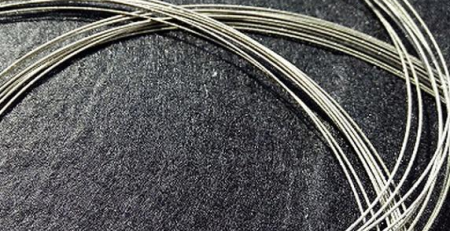
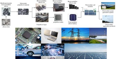
Silicon carbide wafers are single crystal flakes formed by cutting, reibend, polishing and cleaning silicon carbide crystals. Als Halbleitersubstratmaterial, silicon carbide wafers can be made into silicon carbide-based power devices and microwave radio frequency devices through epitaxial growth and device manufacturing. It is an important basic material for the development of the third-generation semiconductor industry.

Siliziumkarbid-Wafer geschnitten SIC Wafer geschnitten mit endloser Diamantdrahtschlaufe
According to the different resistivity, Siliziumkarbid-Wafer können in leitfähige und halbisolierende Wafer unterteilt werden. Darunter auch, conductive silicon carbide wafers are mainly used to manufacture high temperature and high voltage power devices, and the market scale is large; Halbisolierende Siliziumkarbid-Substrate werden hauptsächlich in Mikrowellen-Hochfrequenzgeräten und anderen Bereichen verwendet. Mit dem beschleunigten Aufbau von 5G-Kommunikationsnetzen, the market demand has increased significantly.
Silicon carbide has a wide range of applications
Due to its wide band gap, it can be used to make ultraviolet detectors or blue light diodes that are almost unaffected by sunlight; Its withstand voltage or electric field is 8 times that of silicon and gallium arsenide, and it is especially suitable for the manufacture of high-voltage and high-power devices such as high-voltage diodes, power triodes, and high-power microwave devices.
And has a high saturation electron migration speed, can be made into various high-frequency devices (radio frequency and microwave);
Silicon carbide is a good conductor of heat, and its thermal conductivity is better than any other semiconductor material, which allows silicon carbide devices to work well at high temperatures.

Siliziumcarbid (Sic) is an ideal material for high-power devices and the first-generation basic material for the semiconductor industry. Currently, more than 95% of the world’s integrated circuit components are made of silicon. With the development of applications such as electric vehicles and 5G, the demand for high-power, high-voltage, and high-frequency devices is rapidly increasing.
When the voltage is greater than 900V, the shortcomings of silicon-based power MOSFETs and IGBTs will be exposed, which will be limited in many aspects such as conversion efficiency, switching frequency, and operating temperature.
Siliziumcarbid (Sic) has a large band gap (3 times that of Si), hohe Wärmeleitfähigkeit (3.3 times that of Si or 10 times that of GaAs), high electron saturation mobility (2.5 times that of Si), high breakdown electric field (5 times that of Si or GaAs), etc.
It is widely used in extreme environments such as high temperature, high pressure, high frequency, high power electronic devices, Luft- und Raumfahrt, military industry, and nuclear energy.