炭化ケイ素ウェーハの用途と今後の開発動向
炭化ケイ素ウェーハの用途と今後の開発動向
炭化ケイ素 (ティッカー) パワー半導体産業の主な開発方向です, また、パワーデバイスの製造に使用することで、電力利用率を大幅に向上させることができます. 近い将来, new energy vehicles will be the main application scenarios of silicon carbide power devices.

Compared with traditional silicon materials, 炭化ケイ素は、第3世代の半導体材料の代表格です. 広帯域という特徴があります, 高温耐性, high pressure resistance, high frequency, high power and radiation resistance.
It has the advantages of fast switching speed and high efficiency, which can greatly reduce product power consumption, improve energy conversion efficiency, and reduce product volume. It will be the most widely used base material for making semiconductor chips in the future.
Silicon carbide wafers are single crystal flakes formed by cutting, 研削, polishing and cleaning silicon carbide crystals. 半導体基板材料として, silicon carbide wafers can be made into silicon carbide-based power devices and microwave radio frequency devices through epitaxial growth and device manufacturing. It is an important basic material for the development of the third-generation semiconductor industry.

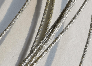
炭化ケイ素ウェーハカット エンドレスダイヤモンドワイヤーループでカットされたSICウェーハ
According to the different resistivity, 炭化ケイ素ウェーハは、導電性タイプと半絶縁タイプに分けることができます. その中で, conductive silicon carbide wafers are mainly used to manufacture high temperature and high voltage power devices, and the market scale is large; 半絶縁炭化ケイ素基板は、主にマイクロ波無線周波数デバイスやその他の分野で使用されています. 5G通信ネットワークの構築が加速, the market demand has increased significantly.
Silicon carbide has a wide range of applications
Due to its wide band gap, it can be used to make ultraviolet detectors or blue light diodes that are almost unaffected by sunlight; Its withstand voltage or electric field is 8 times that of silicon and gallium arsenide, and it is especially suitable for the manufacture of high-voltage and high-power devices such as high-voltage diodes, power triodes, and high-power microwave devices.
And has a high saturation electron migration speed, can be made into various high-frequency devices (radio frequency and microwave);
Silicon carbide is a good conductor of heat, and its thermal conductivity is better than any other semiconductor material, which allows silicon carbide devices to work well at high temperatures.

炭化ケイ素 (ティッカー) is an ideal material for high-power devices and the first-generation basic material for the semiconductor industry. Currently, more than 95% of the world’s integrated circuit components are made of silicon. With the development of applications such as electric vehicles and 5G, the demand for high-power, high-voltage, and high-frequency devices is rapidly increasing.
When the voltage is greater than 900V, the shortcomings of silicon-based power MOSFETs and IGBTs will be exposed, which will be limited in many aspects such as conversion efficiency, switching frequency, and operating temperature.
炭化ケイ素 (ティッカー) has a large band gap (3 times that of Si), 高い熱伝導率 (3.3 times that of Si or 10 times that of GaAs), high electron saturation mobility (2.5 times that of Si), high breakdown electric field (5 times that of Si or GaAs), 等.
It is widely used in extreme environments such as high temperature, high pressure, high frequency, high power electronic devices, 航宇, military industry, and nuclear energy.